And Schematic Diagram With Transistors Npn Pnp Transistors I
Transistor principle electrical4u Npn pnp transistors introduction Mad life: [반도체기초] vcc vdd vee vss
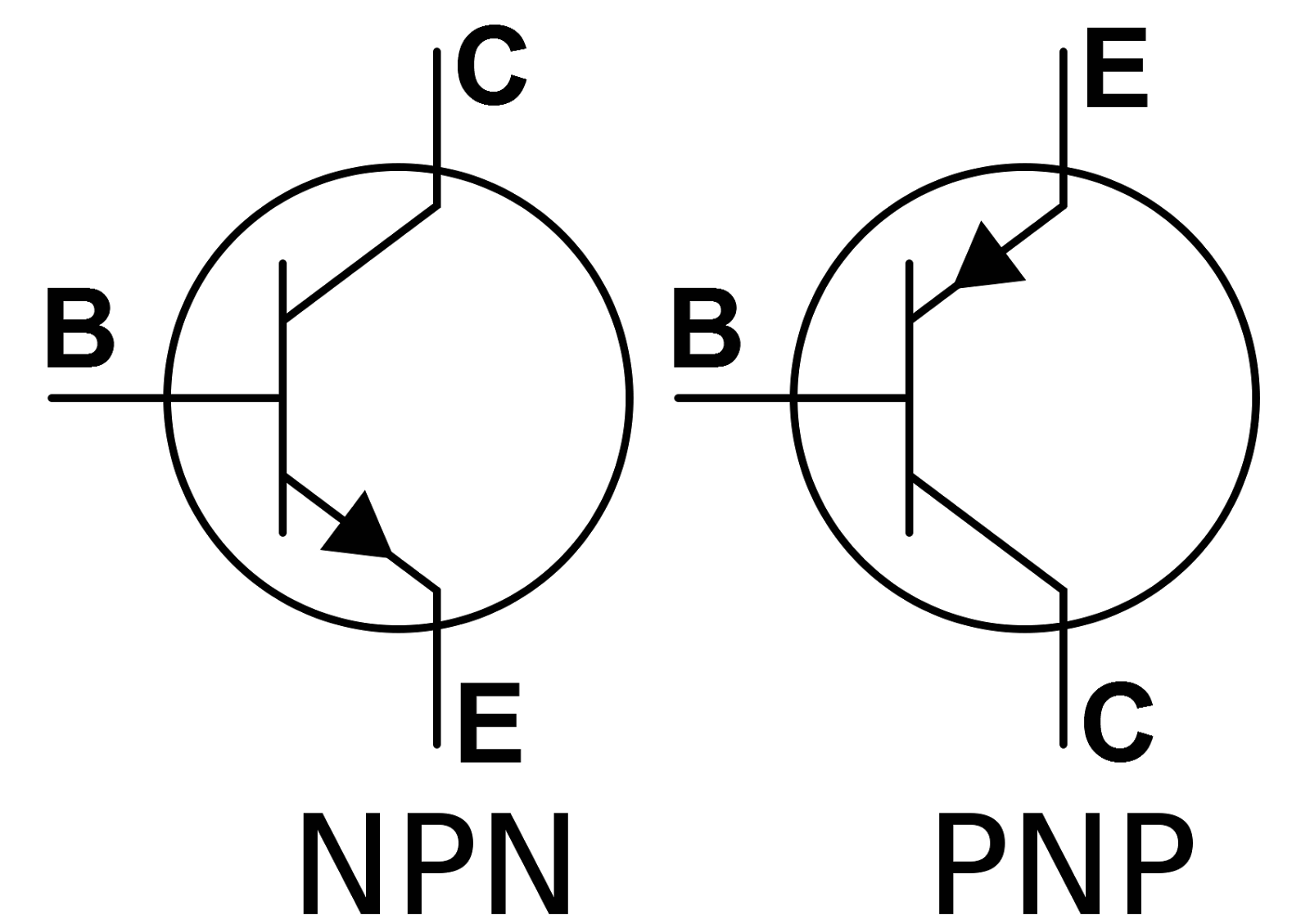
BJT Transistors: Symbol, Basics, Construction, Working & Applications
Transistor basics Transistor pnp circuit characteristics emitter collector symbol base figure schematics common lab modern symbols note 26. transistor characteristics — modern lab experiments documentation
20+ transistor block diagram
Transistor symbols in schematicsTransistors transistor label based polarity methods sometimes inconsistent labeling but Bipolar junction transistorPnp and npn transistor diagram.
Transistor diagram inverter paksc make science d1047 pkTransistor npn circuits wikipedia Transistor transistors explanation npn circuits flows spansTransistor bjt cutoff npn pnp operation saturation active emitter.

How transistor works as switch. npn and pnp transistor working
Transistor pnp work does circuits electronic electronics current npn base emitter voltage explanation difference turn example transistors collector positive negativeTransistor schematic diagram How to calculate total resistance in a bridge circuit using transistorTransistor emitter wiring.
Transistor npnExperiment: transistor circuit design Transistor wiringThe answer is 42!!: september 2012.
Transistor bipolar junction bjt transistors emitter npn
Pnp transistorPower transistor circuit diagram Draw a circuit diagram of the n-p-n transistor with its emitter- baseTransistor basics npn.
Working principle of transistorTransistor: génie électrique Junction transistorElectronic – help with understanding transistors in circuits – valuable.

Transistor pnp npn transistors circuitspedia schéma depuis amplifier
Bjt transistor bipolar junction circuit electronic transistors unit applications components101 circuits understanding rantle controlledTransistors introduction transistor common electronics used bjt bi junction most tutorial Transistor best build guide- how transistors workTransistors npn transistor diagram use base answer diagrams current bmp two used.
Operation of bjt in active,saturation and cutoff regionBjt transistors: symbol, basics, construction, working & applications Transistor diagram 2Electronics basics.

Transistor collector output circuit amplifier experiment emitter common circuits single two wiring experiments ground amplify requirements
File:transistor simple circuit diagram with npn labels.svgTransistor electronic component with its symbol diagram vector .
.

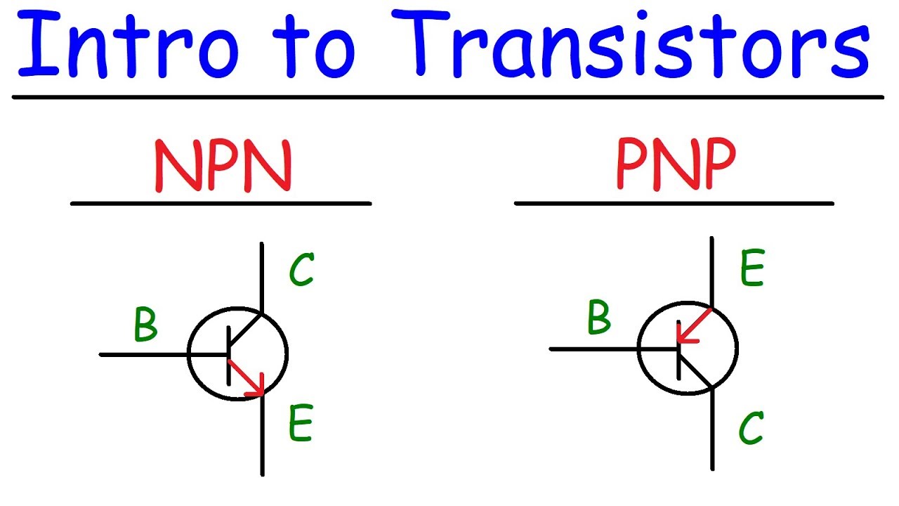
Transistors - NPN & PNP - Basic Introduction - YouTube

Power Transistor Circuit Diagram

BJT Transistors: Symbol, Basics, Construction, Working & Applications
![Mad Life: [반도체기초] Vcc Vdd Vee Vss](https://1.bp.blogspot.com/-GGq7sqgzpY0/VCo56goAExI/AAAAAAAAA-M/GYTbuLBzi6U/s1600/What-is-Transistor-8.png)
Mad Life: [반도체기초] Vcc Vdd Vee Vss

Transistor: Génie électrique

26. Transistor Characteristics — Modern Lab Experiments documentation

Operation of BJT in Active,Saturation And Cutoff Region - Electrical Volt